(China (Mainland))

Product Summary
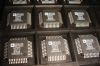
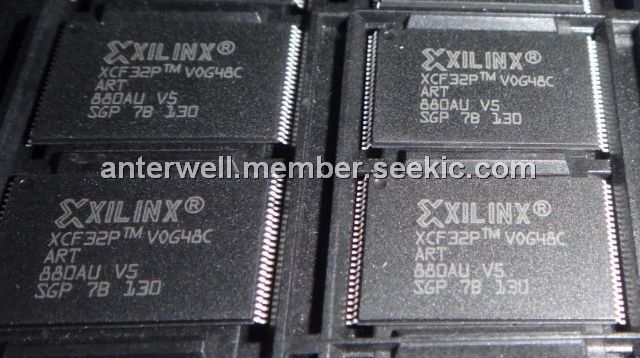
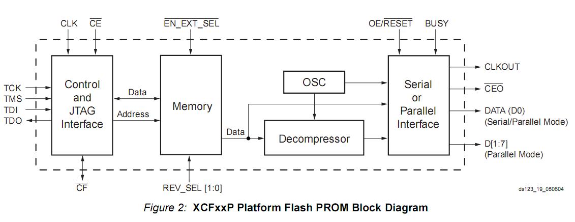
The XCF32PVOG48C is Platform Flash In-System Programmable Configuration PROMS. Available in 1 to 32 Megabit (Mbit) densities, The XCF32PVOG48C provides an easy-to-use, cost-effective, and reprogrammable method for storing large Xilinx FPGA configuration bitstreams. The XCF32PVOG48C includes both the 3.3V XCFxxS PROM and the 1.8V XCFxxP PROM.
Parametrics
XCF32PVOG48C absolute maximum ratings: (1) Internal supply voltage relative to GND (Vccint) : -0.5V to +27V; (2) I/O supply voltage relative to GND (Vcco) : -0.5 to +4.0V; (3)JTAG I/O supply voltage relative to GND (Vccj) : -0.5 to +4.0V; (4) Input voltage with respect to GND (Vin) : -0.5 to +3.6V (Vcco<2.5V) , Vcco≥2.5V; (5) Voltage applied to High-Z output: -0.5 to +3.6V (Vcco<2.5V) , Vcco≥2.5V; (6) Storage temperature (ambient) Tstg: -65°C to 150°C; (7)Junction temperature (Tj) : +125°C.
Features
XCF32PVOG48C features: (1) In-System Programmable PROMs for Configuration of Xilinx FPGAs; (2) Low-Power Advanced CMOS NOR FLASH Process; (3) Endurance of 20,000 Program/Erase Cycles; (4) Operation over Full Industrial Temperature Range (-40°C to +85°C); (5) IEEE Standard 1149.1/1532 Boundary-Scan (JTAG) Support for Programming, Prototyping, and Testing; (6) JTAG Command Initiation of Standard FPGA Configuration; (7) Cascadable for Storing Longer or Multiple Bitstreams; (8) Dedicated Boundary-Scan (JTAG) I/O Power Supply ( Vccj) ; (9) Design Support Using the Xilinx Alliance ISE and Foundation ISE Series Software Packages; (10) Built-in data decompressor compatible with Xilinx advanced compression technology.
Diagrams
 |
 XCF32P |
Other |
|
Data Sheet |
Negotiable |
|
||||